[ INURUM HARDWARE LABS ] SCHEMATICS • MULTI-LAYER • DFM • ATE JIGS

PCB Design & IoT
Hardware Development

We design high-reliability electronic schematics, multi-layer PCB layouts, and RF antenna circuits for IoT devices, automotive systems, and industrial controllers. Engineered in Indore, India for turnkey manufacturing.

[ HARDWARE CAPABILITIES ]

End-to-End PCB Engineering

From initial component selection and power architecture to multi-layer routing, DFM optimization, and automated testing jigs.

Schematics & Multi-Layer Layout

2-layer to 6-layer HDI boards with high-speed differential pairs (USB, Ethernet), signal return path ground planes, and strict power integrity routing.

Altium • KiCad • Controlled Impedance • HDI

RF & Cellular Antenna Design

Impedance-matched 50Ω transmission lines, coplanar waveguides, and integrated PCB trace antennas for 4G LTE, GNSS/GPS, BLE, and Wi-Fi.

50Ω Microstrip • Pi-Matching • GNSS • LTE Cat-1

Automotive & Industrial Protection

TVS surge diodes, reverse polarity protection, optocoupler electrical isolation, and automotive load dump suppression (ISO 7637-2).

Load Dump Protection • Galvanic Isolation • EMI/EMC

DFM & BOM Optimization

Design for Manufacturability (DFM) and Assembly (DFA) audits. We optimize Bill of Materials (BOM) cost with active supply chain sourcing.

SMT Footprints • BOM Lifecycle • Sourcing Strategy

Power Delivery & Battery Mgmt

High-efficiency buck/boost regulators, low-quiescent LDOs, LiPo/LiFePO4 battery charge management, and Power-over-Ethernet (PoE) circuits.

PoE 802.3af • Buck/Boost • Battery Fuel Gauging • LiPo

Automated Factory Test Jigs (ATE)

Custom bed-of-nails testing fixtures equipped with pogo pins, voltage sensors, and automated flashing rigs for reliable mass SMT production.

Pogo Pin Fixtures • Automated QA • Production Flashing
[ REAL PCB DESIGNS ]

Hardware Engineered by Inurum

Inspect the actual multi-layer circuit boards, antenna layouts, and power stages built for our production products.
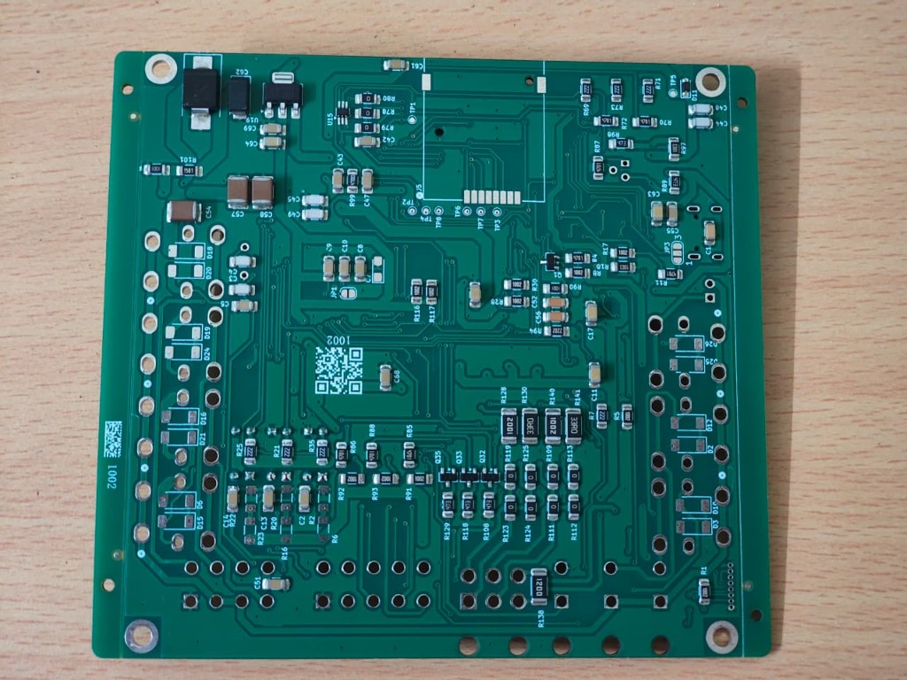
Attendance One Main Control PCB
Enterprise Terminal

Main Controller PCB

Multi-layer control board hosting dual-core processor, flash memory, and peripheral drivers for Attendance One.

View Product
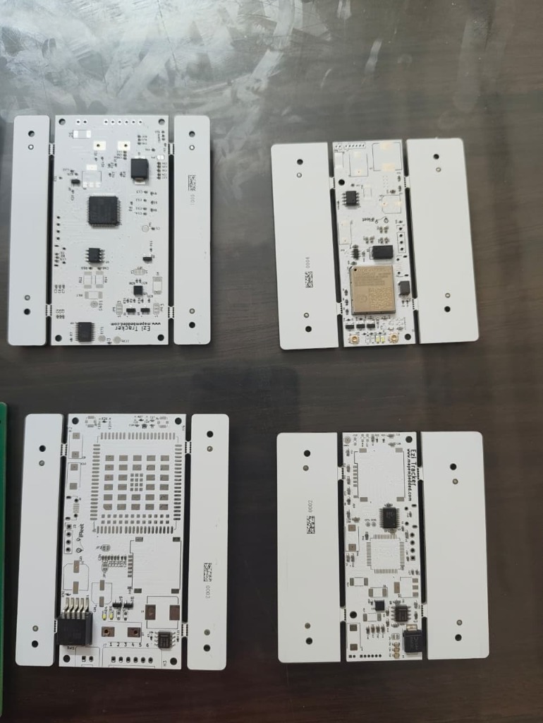
RFID Sensor Grid PCB with Antenna Matching
RF & Sensing

RFID Antenna Layout

Tuned 13.56MHz loop antenna and impedance matching stage for sub-second contactless badge recognition.

View Product
SmartStarter Automotive Telematics Hardware
Commercial Telematics

SmartStarter Controller

Heavy-duty commercial vehicle board with J1939 CAN transceiver, ignition relays, and transient surge filters.

View Case Study
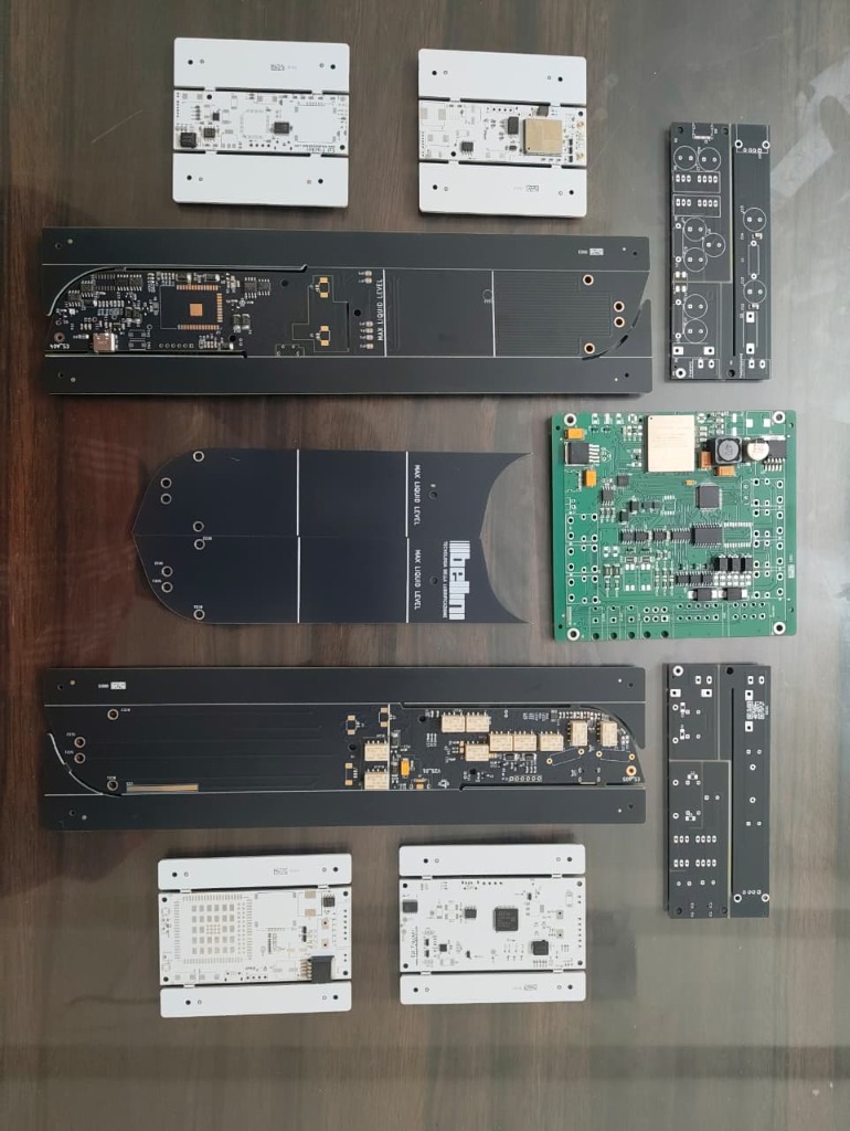
Power & Networking PCB
Power & Comms

Power & Network Module

Isolated DC-DC power supply board with PoE Ethernet PHY interface and transient protection stages.

View Product
[ HARDWARE DESIGN WORKFLOW ]

How We Take Your PCB to Production

PHASE 01

Architecture & BOM Cost

Defining system block diagrams, power budgets, footprint dimensions, and verifying component stock availability.

PHASE 02

Schematic & Multi-Layer Routing

Hierarchical schematic capture, DRC validation, RF impedance matching, thermal vias, and multi-layer ground planes.

PHASE 03

Prototyping & Lab Bring-Up

Bare board fabrication, prototype assembly, oscilloscope signal integrity validation, and power rail stress testing.

PHASE 04

Test Jigs & Mass Assembly

Building functional pogo-pin test fixtures (ATE) and coordinating with SMT assembly lines for volume manufacturing.

[ FREQUENTLY ASKED QUESTIONS ]

PCB Design FAQs

What EDA software tools do you use for schematic capture and PCB layout?
We engineer hardware using industry-standard EDA suites including Altium Designer, KiCad, and EAGLE, delivering clean schematic sheets, modular hierarchical blocks, and verified Gerber RS-274X / IPC-2581 outputs.
Can Inurum design high-density multi-layer boards with RF and cellular antennas?
Yes. We regularly design 2-layer, 4-layer, and 6-layer high-density interconnect (HDI) boards featuring controlled impedance microstrips, RF matching networks for 4G LTE, GPS/GNSS, BLE, and Wi-Fi trace antennas.
How do you ensure Design for Manufacturability (DFM) and component availability?
We conduct thorough DFM/DFA checks against standard fabrication house rules (trace spacing, via aspect ratios, annular rings) and perform BOM lifecycle risk analysis to choose active components with reliable sourcing across Indian and global distributors.
Do we get complete ownership of all design files and Gerbers?
Yes. You retain 100% intellectual property ownership of all schematic captures, layout project files, production Gerbers, drill files, BOMs, and pick-and-place centroid files.
Can Inurum build custom automated testing jigs (ATE) for mass production?
Yes. We design dedicated bed-of-nails functional test jigs (ATE) equipped with automated voltage measurement, current draw verification, and firmware flashing fixtures for factory SMT runs.
[ READY TO BUILD HARDWARE? ]

Turn Your Electronic Concept into Real Hardware

Consult with our hardware engineers in Indore to review your component architecture, schematic drafts, or enclosure constraints.

Request Hardware Consultation Chat on WhatsApp